One does not simply gift cheap Chinese toys to an engineer without expecting them to get taken apart. So, after receiving one of these 168-in-1 digital pets, otherwise known as “Bunnyroms” or generically as “fake Tamagotchis”, I thought I would see what makes it tick.
Note that so far I have only taken the teardown process to a point before it gets destructive. At the end of the page I propose a schematic for the device but there are likely some errors in it which I could only resolve by removing epoxy or sanding down the PCB. If you have experience with these tasks and (for some reason) a desire to fully reverse engineer a Bunnyrom pet, give me a shout!
My Bunnyrom device came from Flying Tiger in the UK, where they retail for £5 and come in a branded box. The same devices are available from a number of sellers on AliExpress and elsewhere, such as this one for around £1 to £1.50.
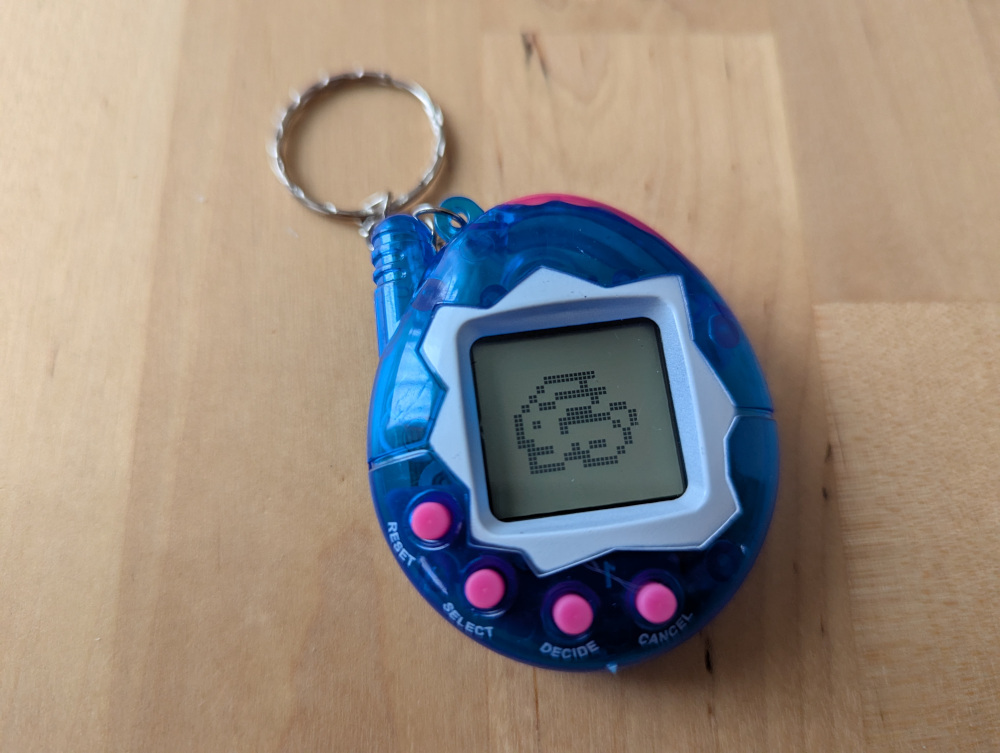
The devices are superficial clones of Tamagotchi virtual pets, with various changes such as being able to select from any of 168 “pets” including copyrighted characters such as SpongeBob. Animations are simpler compared to the Tamagotchi, and there is no evolution or death. My unit has the “egg with antenna” shape used by Tamagotchis with infra-red communication capabilities, but the device does not have any hardware or software support for that.
The Bunnyrom site has a lot of detail on the software itself, plus some photos of the exterior of various devices with this ROM, but I wasn’t able to find a site online that had details of the inner workings. So of course, I decided to figure it out for myself, as far as I could.
The entire device can be disassembled with a small cross-head “watch-maker’s”-type screwdriver. The first and easiest bit to get access to is of course the battery compartment, where two LR44 1.5V batteries sit in series to power the device.
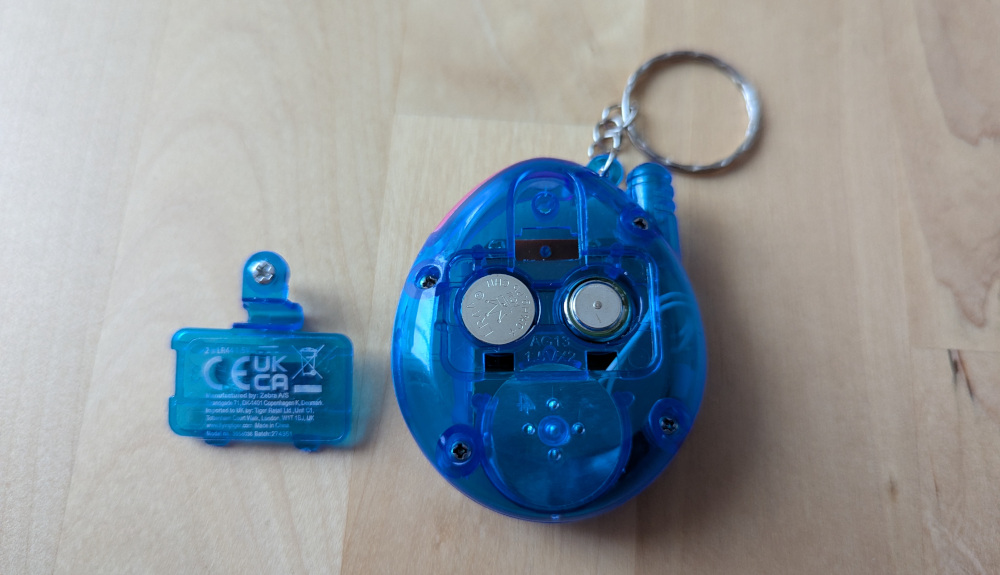
From there, the back of the shell can be removed by taking out four slightly smaller M1 bolts. This allows access to the rear of the PCB, and the piezo buzzer that is fitted to the back of the shell. The buzzer can be lifted out easily by inserting a screwdriver between it and the plastic shell, and levering it gently.
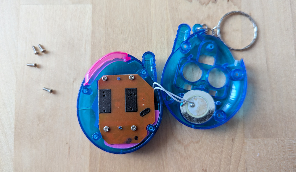
Four more M1 bolts then hold the PCB to the front of the shell. These can be removed just as the previous ones were, but be careful not to mix them up as they are a different length to the previous four.
The PCB and piezo buzzer should now be separate from any of the shell. The screen will likely still be attached to the front of the shell—you can pop this out with a little force by pushing in from the front of the device.
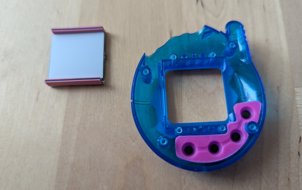
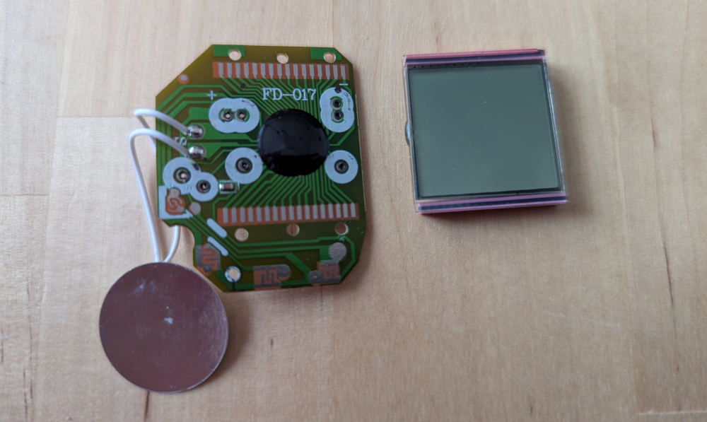
At this point one of the (in my opinion) clever space-saving techniques becomes apparent. There are no connectors on the rear of the screen—the screen is instead pushed in contact with the PCB when the PCB is screwed in, and contacts a set of 32 exposed pads on the board. The four control buttons follow a similar approach, with conductive pads on the bottom of the rubber buttons which close the connection between two close-together exposed pads on the board.
In fact, the only parts protruding from the PCB at all are the microprocessor (sadly covered in epoxy), one tiny surface-mount component, and the soldered-on wires for the buzzer. Everything else is just done with traces and pads on the PCB.
If you lose track of which way round the screen is supposed to be, don’t worry. There is a small tab on one side, which when the screen is the right way up on top of the PCB, should be pointed towards the left-hand side, nearest to the “Reset” button, as shown in the photo below.
The next challenge was to trace the connections between different parts of the PCB (visually, and with a multimeter where possible). Sadly most of the PCB traces are not on an outside layer, and without the ability to remove the epoxy blob over the microprocessor, this was not 100% achievable. A proposed schematic is shown below, but note the following caveats:
- I count somewhere between 41 and 43 traces leaving the “blob”. In the schematic I have assumed a total of 44 for a nice square chip, with pin 44 left disconnected, and some questions about which pins are present in the 38-41 range. This corresponds to the area where a white ring touches the epoxy blob, and therefore it’s very difficult to figure out how many traces emerge underneath it.
- There are some other areas, particularly around the “Reset” button, where the traces are also not that obvious, so some questions remain.
- I’m not 100% sure what the exposed surface mount component is. It doesn’t seem to be resistive, so I have assumed a capacitor. I don’t have the equipment to measure it.
- I also don’t have a logic analyser to attempt to figure out what the display pins are, so I have simply numbered them.
One fun fact about this device is that it seems to require a low-enough current that it can be activated simply by the current supplied by a multimeter in continuity test mode. If you buzz out the battery positive to negative terminals for example, you get a beep—but not from the multimeter—it’s the device itself powering up and playing a sound on its buzzer!
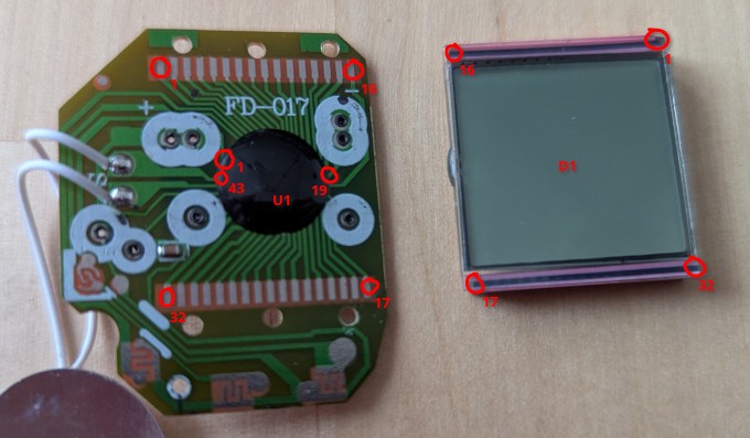
The following photo shows my pin numbering convention. This is not necessarily the convention used by the manufacturer of the microcontroller or screen, but I have not been able to identify either part.
My best guess for the schematic for this device is as follows. Click here to download the KiCAD project.
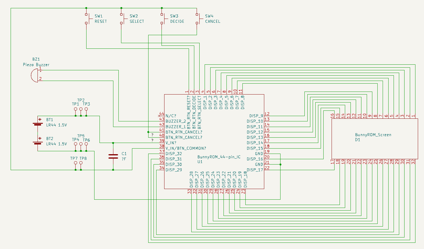
I’m not sure why there are 8 through-hole vias on the PCB. The two that appear with a “+” sign next to them, along with the one immediately below it, are all connected to battery positive and are shown as TP1, TP2 and TP3 on the schematic. On the right-hand side of the PCB, the two with the “-“ sign next to them and the one immediately below them are all connected to battery negative and are shown as TP4, TP5 and TP6. The two that are on a diagonal next to the “Reset” button on the left-hand side are connected to the opposite side of the capacitor compared to 1-3, and are shown as TP7 & TP8.
Sanding off the top layer of the PCB may allow some of the current questions to be resolved, but I’m holding off on this for now as it’s something I’ve not done before, and I am likely to get it wrong and destroy the board!
As for getting any further, I originally wondered if I might discover something like JTAG pads with which the microcontroller could be interrogated and potentially reprogrammed. However, it seems that’s not the case. All the exposed pads have had their connections determined, so any hope of identifying or modifying the microcontroller lies within the epoxy blob. While it is in theory possible to dissolve the epoxy, in non-expert hands like mine this would almost certainly destroy the fragile connections inside.
So that’s it for now—we have some assembly/disassembly photos and a partial schematic. If you are able to provide any more information on these devices, please do get in touch!
Comments